Ruddlesden–Popper phase layered 2D perovskite materials gained importance due to their technologically relevant environmental and photostability compared to their 3D counterpart. The synthesis of layered 2D perovskites with higher n values (n>3), having a broader light absorption, has motivated us to use it as a light absorber in solar cells. This, coupled with our capability to grow highly crystalline Ruddlesden–Popper (RP) layered perovskite thin films using the solution-based Hot-casting technique to obtain a preferential out-of-plane orientation, has enabled photovoltaic cells with power conversion efficiency approaching 13% in a simple planar configuration. In addition, our group demonstrated >2000 hrs of constant solar cell operation in 65% humidity without significant degradation (see Tsai et al. Nature 536 (7616), p. 312, 2016).
Our group has further extended the use of layered 2D Ruddlesden–Popper perovskite in fabricating efficient and stable LEDs with tunable color by a simple solution-processed technique. The as-obtained vertically oriented thin films were observed to facilitate efficient charge injection and transport, enabling an efficient electroluminescence with a high radiance and an ultralow turn-on voltage of 1 V.
Memory seeds to enable phase purity in 2D halide perovskite thin films
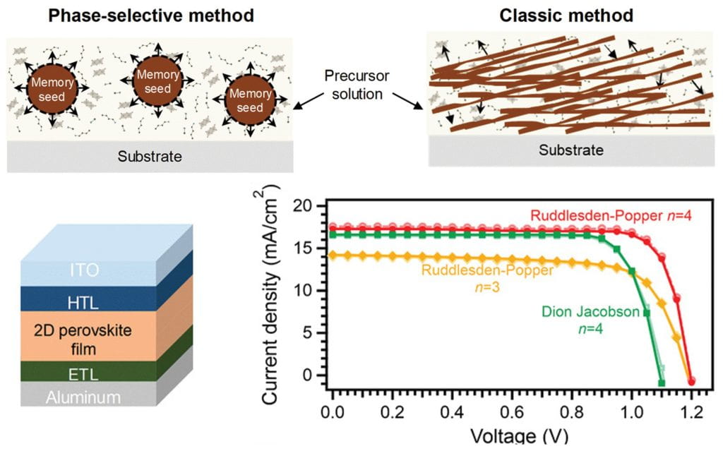
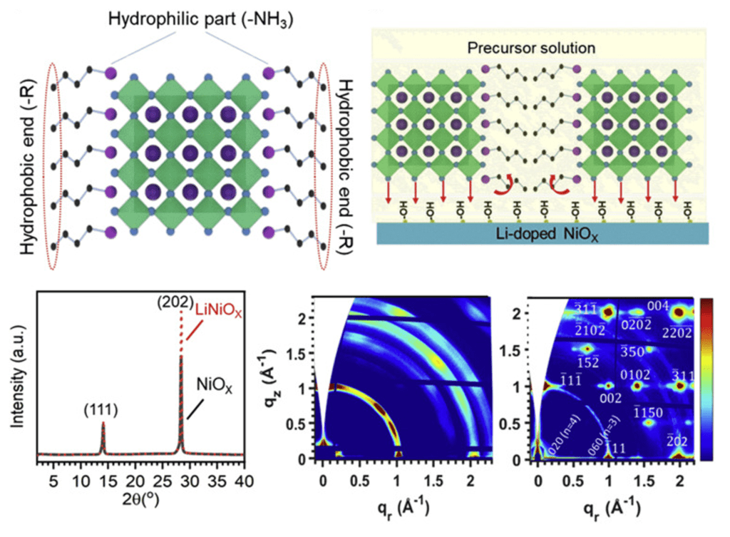
Sidhik et al. developed a novel method to fabricate phase pure films of quasi-2D perovskite using memory seeds synthesis. In this method, 2D perovskite crystals are synthesized and then dissolved in common perovskite solvents like DMF and DMSO. But in comparison to the classical method where precursors of the 2D perovskite are added in stoichiometric quantities, they observe that the memory-seeds process retains a certain memory of the parent dissolved crystal in the form of small crystallite colloids in the solution, which enables the formation of high phase purity films when spin-coated on glass substrates. (Sidhik et al. Adv.Mater.2021, 33, 2007176)
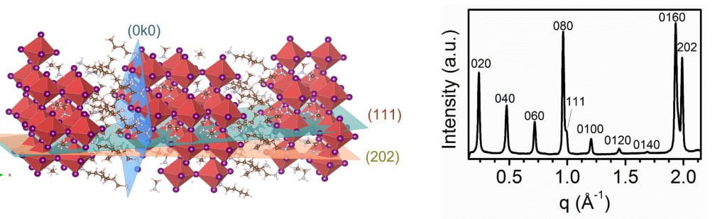
They also observed that the orientation of the 2D perovskite is very important for better charge transport. Orientation along the (0k0) planes blocks charge transport due to the presence of large bulky spacer cations. In contrast, orientation along the (111) and (202) planes improves the charge transport due to channels along the lead-iodine octahedra.
Sidhik et al. then found a way to optimize the interface between the hole transport layer and the perovskite layer by doping a small amount of Lithium nitrate into the nickel oxide precursor solution. This increased the NiO surface’s hydrophilicity by forming new (-OH) hydroxide bonds that attracted the hydrophilic part of the memory seed. This led to an improvement in the orientation of the 2D perovskite, consequently leading to an increase in device efficiency.
(Sidhik et al. Cell Reports Physical Science 2, 100601, October 20, 2021)